
 Aerospace industry
 Semiconductor Industry
 Pharmaceutical & Biotech Industry
 Heat Exchanger Manufacturing
 Food & Beverage Industry
 Renewable Energy
 Cooling systems for data centers








The role of stainless steel and innovative welding technologies – an overview of the semiconductor industry in Italy
In 2025, the global semiconductor industry remains robust, driven by strong demand in areas such as artificial intelligence and electric vehicles. The recent chip shortage and geopolitical tensions have prompted governments to invest more heavily in local production of these components. In Europe, the EU Chips Act is mobilizing billions to support domestic manufacturing. Italy has positioned itself as a key player, offering significant incentives to attract chipmakers. For example, €3.2 billion is being invested in Novara in a state-of-the-art facility for advanced chip packaging, while a €5 billion silicon carbide (SiC) chip plant is being built in Catania.
Italy’s strategy therefore focuses on specialized niches where the country can contribute without having to compete directly with global conglomerates. However, the expansion of this sector faces challenges, such as a shortage of skilled workers and infrastructure constraints.
Overall, Italy is experiencing a boom in the chip industry, and thanks to strong government support, the country is increasingly establishing itself within the European semiconductor supply chain. These developments also benefit related industries, including the stainless steel sector, which supplies materials and equipment for new high-tech factories.
Stainless steel in semiconductor manufacturing
Stainless steel is ubiquitous in semiconductor manufacturing – and for good reason. In chip factories (“fabs”), many tools and infrastructure elements are made of stainless steel because it is particularly easy to clean and corrosion-resistant. Austenitic materials such as EN 1.4307 (AISI 304L) and EN 1.4404 (AISI 316L) are especially popular due to their strength and the ability to polish them to a very low surface roughness. Stainless steel is considered inert because it does not corrode and does not release particles, helping to prevent contamination of sensitive processes.

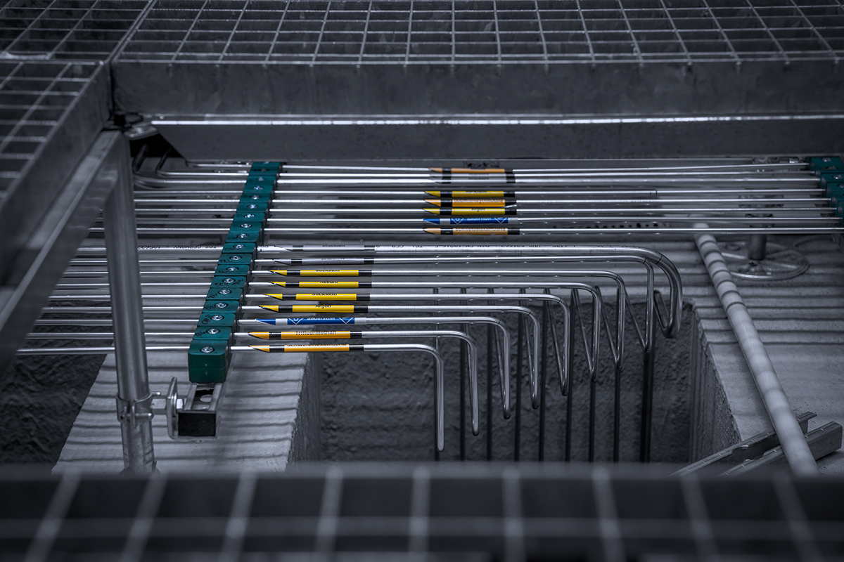
Below is an overview of the entire chip manufacturing process in which stainless steel is used:
- Vacuum process chambers: Reactors and chambers for processes such as deposition and etching are often made of stainless steel. Materials such as AISI 304L or AISI 316L are used because they maintain their integrity under vacuum and can be treated at high temperatures to remove contaminants.
- Gas supply and chemical handling: Piping for high-purity gases, valves, tanks, and acid pumps are made of AISI 316L stainless steel due to its excellent corrosion resistance.
- Cleanroom equipment and facilities: From wafer transport containers to worktables and cabinets, stainless steel is the preferred material for cleanrooms. It is easy to sterilize and does not introduce particles or contaminants into the environment.
With the construction of new facilities and equipment worldwide, demand for high-quality stainless steel components continues to grow steadily. This trend offers the stainless steel industry significant opportunities to contribute to this high-tech manufacturing sector.
Orbital welding of Valve Manifold Boxes (VMBs) in semiconductor gas systems
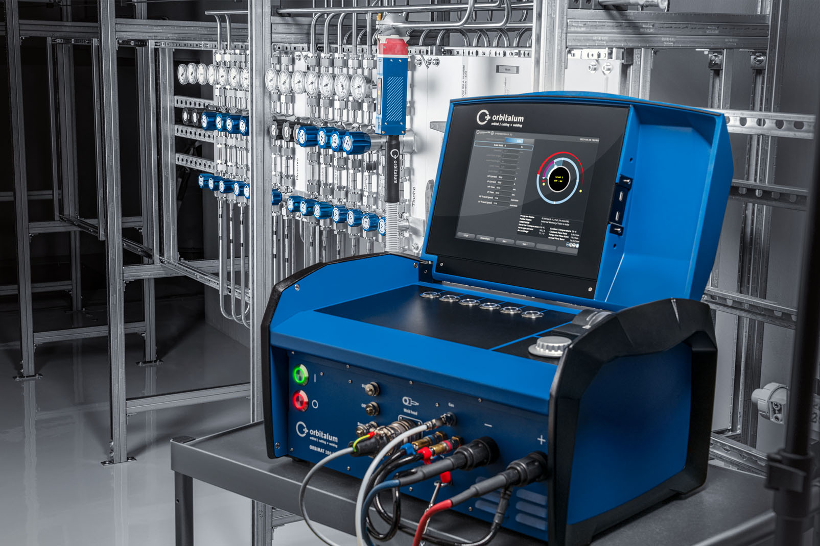
Orbital welding is an automated welding process in which the arc moves 360° around a stationary tube or pipe, producing extremely consistent and precise welds. Orbital arc welding (GTAW/TIG) is frequently used to assemble gas distribution systems for high-purity gases. A key application is the construction of Valve Manifold Boxes (VMBs). These are specialized panels or enclosures used to safely split and control the gas flow from a source to multiple points of use (or, in some cases, to mix multiple gases).
VMBs are widely used in semiconductor fabs, but they are also used in the pharmaceutical industry and other sectors with stringent requirements for clean gas distribution. The enclosure is typically a ventilated cabinet (often connected to an exhaust system) that contains a series of valves and regulators. VMBs enable operators to control gas distribution centrally instead of providing separate gas sources for each tool, improving system efficiency and safety.
Orbital welding for high-purity gas lines
In semiconductor gas distribution, weld quality is critical. Stainless steel tubes (often AISI 316L) have an electropolished inner surface and must be joined with full penetration, without internal gaps where contaminants could accumulate. Orbital welding is the optimal technique for this: it enables a uniform weld with minimal internal bead formation. To prevent oxidation, high-purity argon is used, which simultaneously displaces oxygen inside the tube.
Gas lines in VMBs are typically made from seamless AISI 316L tubing. Industry standards such as SEMI F16 and F17 define the quality requirements for stainless steel tubing used in the semiconductor industry, including electropolished surfaces.
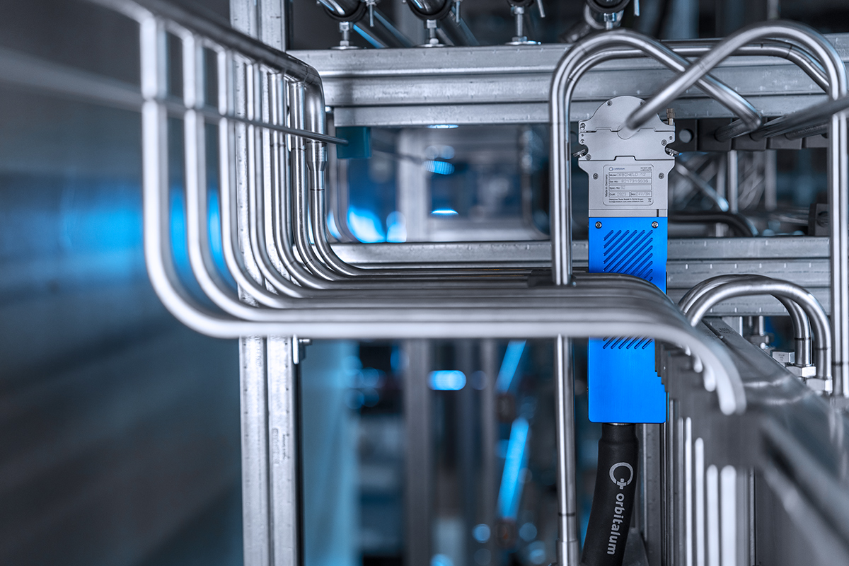
Common tube sizes range from 1/4″, 3/8″ to 1/2″ outside diameter (OD) for individual process gas lines, with relatively thin wall thicknesses (e.g., 0.035″ to 0.065″) to enable proper full-penetration welds during orbital welding. All tube joints in a VMB are typically made as butt welds using orbital GTAW: the tube ends or tube fittings are cut square, aligned, and welded around the circumference. This orbital butt-weld design minimizes the number of threaded or mechanical connections, thereby reducing potential leak and contamination points.
Materials, standards, and quality requirements
Manufacturing VMBs for semiconductor gas applications requires compliance with strict quality and purity standards. Numerous industry standards provide guidance on material selection, welding procedures, and inspection requirements. Semiconductor Equipment and Materials International (SEMI) publishes specific specifications for semiconductor manufacturing equipment. For example, SEMI F3 is a guideline for welding stainless steel tubing in such applications, while SEMI F1 defines requirements for the leak tightness of high-purity gas piping systems and components.
These standards emphasize the use of appropriate procedures (such as orbital GTAW with adequate purging) and achieving extremely low leak rates in finished systems. In addition, the SEMI guidelines address requirements for surface quality and the material condition of the tubing (e.g., SEMI F16/F17 for electropolished AISI 316L tubing) as well as aspects of system design (SEMI F22 as a guideline for gas distribution systems).
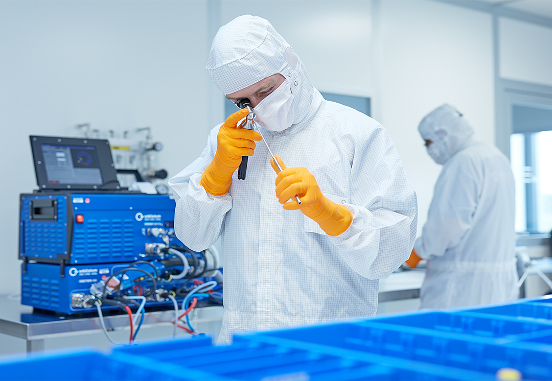
In practice, many VMB manufacturers have their welders certified in accordance with ASME Section IX, qualifying welding procedures and operators. This ensures that welders can produce leak-tight welded joints on tubing of various sizes and materials. Visual inspection of all welds is mandatory, and a certain percentage is often additionally checked using advanced inspection methods to ensure quality.
Conclusion
For professionals in the stainless steel industry, manufacturing valve manifold boxes is a fascinating precision application. It demonstrates how stainless steel, combined with modern welding technology (orbital GTAW), can meet the complex requirements of semiconductor manufacturing.